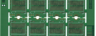
HDI/Microvia PCB

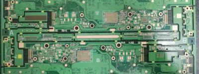
Anylayer HDI PCB
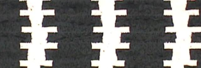
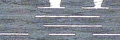
Anylayer HDI PCB Cross Section

Product Type: Anylayer HDI PCB
Application: SSD
Board Layer Structure: 10L
Product Design:

  • Line width/space:2.5/3.5mil
  • Via Filling
  • Selective ENIG
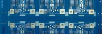
HDI PCB
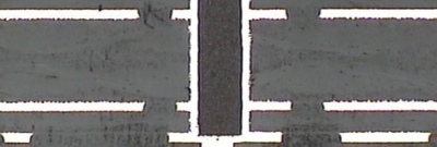
HDI PCB Cross Section

Product Type: HDI PCB
Application: SSD
Board Layer Structure: 8L(2+4+2 structure)
Product Design:

  • Via Filling
  • Stacked Via on IVH
  • Plug Resin in IVH
  • 2 times of Plating on IVH
nh40021-5
HDI PCB cross section 2

Product Type: HDI PCB
Application: Computer
Board Layer Structure: 10L(2+6BV+2)
Product Design:

  • Line width/space:2.36/2.36mil
  • Pad to line 2.36mil

Compared to standard multilayer PCBs, High Density Interconnect (HDI) printed circuit boards feature finer conductive path structures and smaller vias. This is the technological response of the PCB industry to permanent miniaturization that requires more and more complex circuits and components with extremely high pin count.

Laminating more PCB layers in Sequential Build Up (SBU) technology enables interconnection and routing of inner layers without consuming surface area, which can thus be used to place and interconnect high pin count components.

CERTIFICATES

  • ISO 9001:2008
  • ISO 9001:2015
  • ISO 14001:2004
  • ISO 14001:2015
  • OHSAS 18001:2007
  • ISO/TS 16949:2009
  • QC080000:2012 / RoHS
  • VDA6.3
  • EICC
  • TOSHMS
  • CQC

  • 27. Feb 2017